
XMG Apex 15 Laptop: DRAM Memory Overclocking
[Original source] Partially based on the script of my YouTube videos: https://www.youtube.com/watch?v=qCkNcZ6WEQQ and https://www.youtube.com/watch?v=RWVm1_JCTEo
[Updated] Contains updated data from 2021.
This guide is made for the the following laptops.
[Laptop] XMG Apex 15 Max (2022) with B550 chipset & XMG Apex 15 (2020) with B450 chipset
[Barebone] Clevo NH50VR / NH55VR / NH57VR / NH58VR (B550) & Clevo NH50AF1 / NH55AF1 / NH57AF1 / NH58AF1 (B450)
[Similar laptops] One K56-AR, Eluktronics Thicc-15, Eurocom Nightsky ARX15
[CPU] Zen3 & Zen2 Ryzen Desktop CPUs
[Note] This guide is applicable for Zen3 and Zen2 Ryzen CPUs in the B550 chipset based XMG APEX Max (E22) and B450 chipset based XMG APEX (E20) laptop.
[MHz is marketing] I will talk about DDR4 DRAM frequencies like 2666 MHz or 3200 MHz in this post, but I want to note that the term of “MHz” is wrong in this context, since 3200″MHz” modules run at 1600 MHz in reality. The “MHz” are a marketing term, which is why I will use quotation marks when I am using this “every day” language in this post. 🙂
Introduction
Today I will talk about memory overclocking and some basics like memory characteristics, possible performance gains, overclocking tools, and I will show you how to overclock your DRAM in your XMG APEX 15 laptop. But this should also be applicable for most desktop Ryzen systems of course.
I will use the original slow-ish Corsair 2666″MHz” memory sticks my XMG Apex 15 came with. I bet you will be suprised about the results. At least I was.
I had a lot of struggle while making this video (script), because I always felt – and still do – that there is so much more about RAM tuning to analyze. There are so many parameters, so many things which are not obvious how they work and what they influence in which way. If they even influence the results in a measureable way, or if it‘s just “noise” and measuring tolerances. So, sorry I can’t cover all aspects, but I can try to provide a simple guide on how to tune your memory on the Apex 15 with Zen2 and Zen3 processors. Maybe even every AM4 mainboard using a desktop Zen2 or Zen3 processor.
The benefit should be an increased data throughput for the CPU, which ultimately means shorter computation times and more performance in production applications and games.
To gather the data I used three different memory sticks in their JEDEC standard speed and overclocked with tighter timings. The idea was to present you the original out-of-the-box JEDEC default performance and potential performance after investing some time into memory tuning.
Hint: In case you don’t want to read trough all that at first, you can find the results at the end of the article.
Memory sticks used
I used four different memory sticks by two well-known brands and a not so well-known one. Two of them are single rank and the other two are dual rank sticks.
| Product | Default (SPD) Timings | XMP Profile | Size | Rank | Memory IC |
|---|---|---|---|---|---|
| Corsair Vengeance 2666MHz CL18 (16GB kit) | 2666 MT/s CL18-19-19-39-58-467 | – | 2x8GB (16GB) | single rank | Samsung B-die 8-Gbit |
| Corsair Vengeance 2666MHz CL18 (32GB kit) | 2666 MT/s CL18-19-19-39-58-467 | – | 2x16GB (32GB) | dual rank | Samsung B-die 8-Gbit |
| G.Skill Ripjaws 3200MHZ CL18 (32GB kit) | 2400 MT/s CL17-17-17-39-56-421 | yes (3200 MT/s CL18) | 2x16GB (32GB) | dual rank | SKHynix CJR 8-Gbit |
| Oloy Lightning Gaming 3200MHz CL18 (32GB kit) | 3200 MT/s CL18-20-20-40-74-800 | – | 2x16GB (32GB) | single rank | unknown 16-Gbit |
I am happy to have both a single rank and a dual rank Corsair Memory Kit, which uses the very same memory ICs (chips, dies). This way I can test the behaviour of single rank versus dual rank memory more correctly.
Disclaimer: Please note that these modules were bought in the year 2020 and 2021. In the meantime those products could have been updated and use different memory ICs by now. Manufacturers tend to use 16-bit memory ICs in their updated product lines nowadays. That means you possibly can’t get your hands on the very same memory sticks I have anymore.
What about the ranks?
You may ask yourself what single rank (SR) and dual rank (DR) is? It’s the population of the memory chip banks on one memory stick itself. You can fill a memory stick’s available memory data transfer lines by half or fully. By half, or single rank, usually means it’s equipped with memory chips on only one side of the stick. But that’s not always the case. Some memory sticks got their chips on both sides but are still single ranked. Dual rank sticks populate all available data lines on the memory stick.
So I think you can already guess that it’s a disadvantage when you do not use all available data lines, right? In general a dual rank stick will always allow faster memory access, because when one rank of the memory stick is in use the other rank can be prepared for memory actions in the meantime. This basically allows the memory dies to be used in a more parallel way and saves a little bit more time to access data. That’s it. And that’s also the main reason why an untuned (not overclocked) dual rank memory stick will always be faster than a single rank stick.
The only disadvantage of a dual rank stick is that it puts more load on your CPU’s memory controller and usually leads to slightly worse memory timings when you overclock your memory sticks. In my case my dual rank timings were almost always one tick worse, so 3200CL18 for dual rank instead of 3200CL17 for single rank for example. But because dual rank can access data in a more parallel way and is more “time-efficient” the effect is negligible. Even better, usually CL18 dual rank memory is faster than CL17 single rank one.
What about the memory ICs?
Every memory IC behaves a little different. The infamous Samsung B-die for example is well-known to be good in overclocking, but tends to be very temperature sensitive. The SKhynix CJRs should be perfectly made for overclocking, too, but use totally different timing “patterns” than the Samsung B-dies. CJR’s timings tend to be more irregular, while the B-die timings look more homogenous. But that doesn’t hurt performance in any way!
Both of them are 8-Gbit dies, which basically means that there is less storage inside one chip. Memory sticks got a lot of such chips on them. And if you use 8-GBit chips you need all the space you got to fill up a single 16 GB stick. Because we got 8-GBit per chip, which is 1GByte (1GB) we need 16 of such memory chips to make up a 16GB memory stick. This ultimately means for SODIMMs (laptop DRAM sticks) that there is just enough space for 16 of the 8-GBit memory ICs. So we do max out at 16GB memory sticks using 8-GBit memory ICs.
But nowadays we sometimes want more than just 2x16GB (32GB) in total in our computers. So the manufacturers had to introduce 16-GBit chips, which can hold 2GByte (2GB) of data in one chip. This way there is more space on the memory stick left which makes it possible to produce 32GB memory sticks to offer 2x32GB (64GB) DRAM memory configurations.
In general those 16-GBit memory ICs got somewhat worse timings than their older 8-GBit counterparts, because the silicon had to shrink to make the extra data storage fit into it. But this situation should improve with more modern DDR4 memory ICs coming out. Even if it’s the end of the DDR4 era, there are still new well-overclockable ICs coming out which will ultimately find their way into every market segment (desktop DIMM & laptop SODIMM).
–
How can I find out which memory IC is used in a product?
The bad news: there is no way, unless the manufacturer wants to make it public. Most don’t. After all there is no guarantee which memory ICs you will end up with. You can try to find informations in beforehand, but that can also be hard though. I always try to search for terms like “thaiphoon sodimm corsair vengeance 2666” or the product number of the sticks you want to buy together with the term “thaiphoon”. Why Thaiphoon? Well there is a tool called thaiphoon burner, which got the ability to read detailed informations out of the memory IC and finally compares it with a database. This way you can find out which memory IC your or some elses memory stick is using in most cases. But some people report about wrong readings from time to time, so be careful. No guarantee again.
But don’t give up yet. A very active member of the XMG & Friends Discord named “_L_” told me about a useful reddit post, which summarizes some serial numbers of common memory sticks to detect which chips are possibly installed. You can check out the reddit post here: https://www.reddit.com/r/overclocking/wiki/ram/ddr4#wiki_corsair
As you can see in the screenshot down below i read out the details for one of the memory sticks used in this article, the G.Skill Ripjaws F4-3200C18-16GRS DDR4 SODIMM memory sticks.
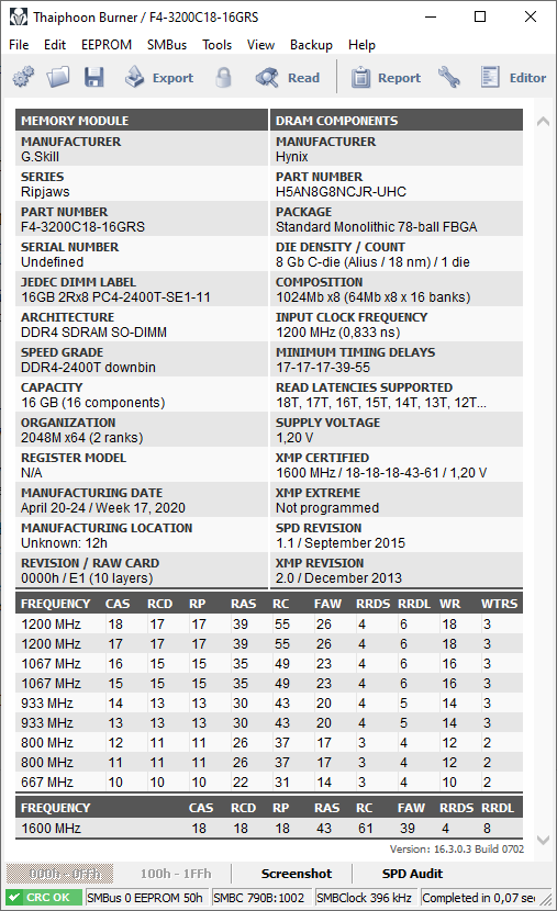
The data in the screenshot tells us a lot about the memory stick’s ICs.
Using the part number (on the right side) you could check if the tool read the correct information. If you remove the sticker on your DDR4 memory stick (and void it’s warranty this way) you should see an imprint on the memory IC. It should match the part number reading. The second part number (on the left side) is the official products part number of the whole stick. You should find this one in the internet too.
The Die Density / Count reading should give you the most important information about the individual chips soldered on the sticks themself. In my case it’s a 8Gbit C-die (CJR) produced in 18nm by Hynix.
And finally the Organization on the left side should give you the information if one memory stick is a single rank (1 rank) or dual rank (2 ranks) stick.
As you can see in the screenshot my sticks were produced in April 2020.
–
Another useful tool: DRAM Calculator for Ryzen by 1usmus
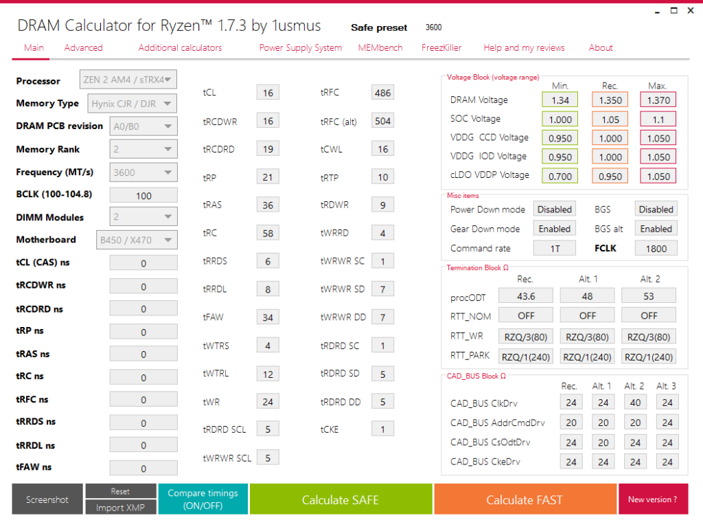
Before we can start I need to tell you about another very useful tool. It’s the DRAM calculator by 1usmus, a well-known name in the overclocking community. He also made the lately known ClockTuner for Ryzen (for Zen2) and the new Project Hydra (for Zen3). All of his tools are free, except the new Project Hydra, which comes in a free and pro version which unlocks more features. But more on that in another post at another time.

On the left side you set your basic computer stats. In the case of the XMG APEX 15 laptop in combination with a Zen2 or Zen3 CPU you can set the values as seen in the screenshot.
The only difference you have to set individually is the Memory Type and the Memory Rank according to your results from Thaiphoon Burner.
Hint: Zen3 CPUs behave pretty much the same as Zen2 CPUs because they share the same memory controller. So you can use the values shown for a Zen2 CPU with a Zen3 CPU, too.
Now after you have made your basic settings click on the green “Calculate SAFE” button. The values which appear for the timings are safe values in the case you can set 1.35V DRAM voltage. But in the case of the XMG APEX 15 we have a fixed DRAM memory voltage of 1.25V… Yes, one-point-two-five, not 1.20V as many people quote. The JEDEC (default) voltage for DDR4 DRAM is 1.2V, but the ODM Clevo decided to push up the voltage a bit by default to increase stability over a wide range of DDR4 SODIMM DRAM. This way we got a little extra overclocking headroom, but the shown values for 1.35V DRAM voltage are unrealistic and very likely unstable.
All other values on the right (expect DRAM voltage) are fine by the way. Remember that for later.
Now, we can’t tell the tool to show us values for just 1.25V DRAM voltage. BUT we can make use of a little trick to find a little more realistic values.
The trick is to investigate the changes of the most important timings for higher DRAM frequency (MT/s) than the one we want. For example, if we look for some values for 3200″MHz” I would look how the timings change when we choose 3466 and 3600″MHz”.
This way we can try to find a “pattern” in the behaviour of the timings over a wider range of DRAM frequencies (MT/s).
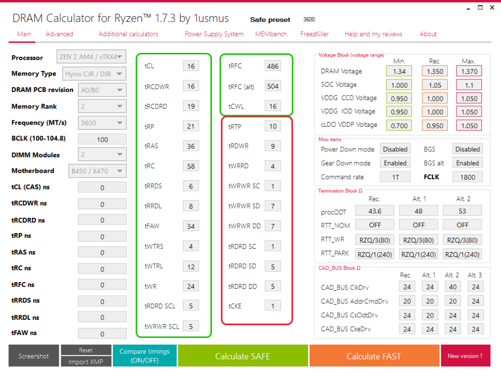
In our example, with the G.Skill Ripjaws modules and their Hynix CJR, we can see that the the tCL (CAS latency) does not really change over the frequency range. The tRCDWR (row-column delay write) does not really change, too. But the tRCDRD (row-column delay read) and tRP (row precharge) change dramatically. Those are the four most important timings which form the “pattern” I was talking about. For those four timings namely tCL, tRCDWR, tRCDRD and tRP we ALWAYS need to take the pattern in mind.
In this example my memory sticks with Hynix CJR dies always need tCL+3 ticks on the tRCDRD timing and tCL+5 for tRP. This is the pattern I am talking about. We need to remember this pattern if we want to find stable timings for even higher DRAM frequencies later on. For example 3466″MHz”, 3600″MHz”, or even 3800″MHz”. I will talk about that “Translation of memory timings for higher DRAM frequencies” in the very end.
Some of the other timings next to those main four follow some rules which allow us to find their absolut limits according to the pattern we found in the four main ones.
The lowest value for tRAS is tRCDRD + tCL, which is 19+16 = 35 in this example. The shown value of 36 is close enough and yes, it’s always wise to plan in some tolerance and plan in slightly higher timings than the limits by calculation.
The lowest value for tRC (row cycle) is tRP + tRAS, which is 21+36 = 57 in this example. Mind the tolerance again and never start at the limit as I said. I would suggest to add at least 5 ticks to tRAS and tRC in the beginning and tighten them later.
All those 6 together influence the DRAM latency by a lot. They are also known as the primary timings.
After the important 6 primary timings, let’s take a look at the very important secondary timings, too.
With the first two secondary timings tRRDS and tRRDL it is usually safe to start at 6 and 8. But most good memory ICs also can run 4 and 6 stable without any problems.
In direct dependence to them is tFAW, which should be between four and six times tRRDS, so in this example between 24 and 36. A good “most times stable” value is five times tRRDS in my experience, so 30 should be working fine. But better start with 6 times here, so 36 in this example.
Those three also got a noticable impact on the overall latency.
Now tWR is more or less bound to tCWL on the right side, so let’s take both into account. They can have a noticable impact on latency.
The timing tCWL (CAS write latency) is bound to tCL as the name suggest. It must be an even number and is equal or one less than tCL.
The timing tWR can be equal or a little less than tCWL. So if you use a tCWL of 18 you are safe to start with a tWR of 18, too. However the absolut safe value for tWR is 24, the lower limit is 12.
The timings tRDRD SCL and tWRWR SCL got a noticable impact on latency again. In my experience it is safe to start with 5 for both timings straight away, but do be sure better start with 6. Use always the same value for both. I have never seen non-equal values for a Ryzen system. But don’t expect to tune much here. Usually you max out at 4.
Let’s switch to the top right side of the table again and talk about a timing which can give you a very noticable impact on latency. Namely tRFC.
But it looks like to be tightly tied to the DRAM voltage. The higher the voltage the lower tRFC can be. This timing controls the time window which is used to refresh the electrical charge inside the storage cells (where the bits are saved). The lower the time window the shorter the voltage can be recharged and the more likely memory corruption gets. This way it makes sense that a higher DRAM voltage allows lower values here.
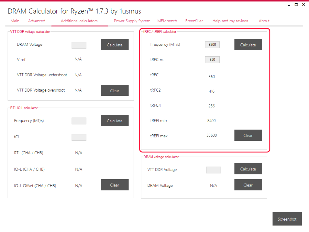
Almost ever the tRFC values the tool is suggesting as safe for us are not safe at all in our constrained DRAM voltage scenario. We should always start at the JEDEC standard 350ns, maybe even 375ns (i had a stick which was not all-time stable at 350ns once). But wait, 350ns are not ticks we can just use! On the third tab called “Additional calculators” there is a tool which allows you to calculate the corresponding tRFC values for a time window given. In our example 350ns corresponds to a tRFC of 560 ticks.
And finally let’s talk about the last timings on the right side. I marked them with a red rectangle in the following image. They mostly do not influence the overall latency by too much. They can be called the tertiary timings and most of them do not follow special rules. But they are important for stability, so don’t stress them too much. In my experience the values suggested by the DRAM Calculator for Ryzen by 1usmus are working fine out of the box in most cases. Even at our lower DRAM voltage. So let’s scan over them quickly.
tRTP can be between 8 and 12. A safe start is 12, a good settle point is 10.
tRDWR and tWRRD can be stable using the “safe settings” preset the DRAM calculator tool suggests for your target DRAM frequency, but I recommend to add another +1 to them to make sure it is stable. Or you check out the suggested values for a ~400MT/s higher DRAM frequency again as I said earlier. So if you want to find values for 3200″MHz” check out the suggested values at 3600″MHz” in the tool. By the way, I told you about tertiary timings do not influence the latency by too much? Well if you want to squeeze out a little bit more tRDWR and tWRRD are worth taking a look at. They are the only two with some impact of all tertiaries. But too low values can lead to instabilities quickly.
All other values usually need no special attention and can be copied from the DRAM calculator for Ryzen tool.
tWRWR SC is usually always 1.
tWRWR SD and tWRWR DD always are equal to each other.
tRDRD SC is usually always 1.
tRDRD SD and tRDRD DD are just like their WRWR counterpartrs always equal to each other.
And finally tCKE does not have any effect in my experience. By default most sticks set it to 7 or 8, but in almost all cases you can set it to 1 straight away and it will work fine. But because it got no measurable influence on latency if it’s at 7 or 1, you can leave it as is to make sure it doesn’t lead to instabilities after all.
Oof, that was a lot of information, right? So I don’t want to continue to stress you too much and come to the end ASAP.
Apply the values via Ryzen Master
AMD’s Ryzen Master is a tool to gain some control over the behaviour of your Ryzen system. It also allows you to create different profiles which also include DRAM overclocking. And that’s exactly what we will use. The changes made here are permanently “copied into the BIOS” and you do not need to apply them over and over again after a reboot.
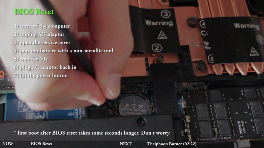
In case you fail: Reset the BIOS
If your settings fail to boot you can always reset your BIOS by unplugging the AC adapter (DC jack), taking out the lithium battery and finally also the CMOS battery, which you can find under the service lid in between your M.2 SSDs and the DDR4 SODIMMs. Use a !non-metallic! tool to push it gently sidewards and pop it out. Wait for 60 seconds and re-plug at least the AC adapter and boot up the laptop. Don’t panic, the first boot after a BIOS reset will take a 10-30 seconds longer than usual.
Now, create a profile in Ryzen Master and apply the settings.
Set your Memory Clock to HALF of the DRAM frequency you want to use. Why half? Because it’s called DDR memory = double data rate. So the whole 3200″MHz” thing is a lie and it runs at 1600MHz in reality. It’s called “3200 MHz” anyway because it behaves “effectively” like 3200 MHz memory due to it’s double data rate. A more correct naming would be “3200 Megatransfers per second” memory, or 3200 MT/s as found in enthusiast software. But marketing does not like that, so we are all used to the strange “effective” marketing values.
Set your VDDCR SOC voltage to 1.025V (safe value) for 3200 MT/s (real 1600MHz Memory Clock), 1.050V for 3466 MT/s (real 1733MHz Memory Clock) and 1.075V for 3600 MT/s (real 1800MHz Memory Clock). You can lower those values later and see if it’s still stable and the performance does not drop. A lower VDDCR SOC voltage reduces the overall power draw of the SOC and leaves more CPU package power headroom for the cores. A too low VDDCR SOC voltage can lead to performance degradation. Check popular CPU benchmarks and compare your results of !multiple! runs to see if you loose any performance when you lower this voltage.
CLDO VDDP and CLDO VDDG can usually be set to 0.900V safely. Both voltages depend on VDDCR SOC and need to be at least 50mV (0.05V) lower than VDDCR SOC.
Next up is the “copy and pasting” of the timings found using my description from before (heading: “Another useful tool: DRAM Calculator for Ryzen by Yuri Bublii (1usmus)”). Remember to follow this little manual, the suggested values by the tool will not work without adjustments.
The only thing I need to notice is that Ryzen Master names some of the timings a little bit differently. The software does not use the short name, it does use the full technical name for some of the timings. Let me clarify which one is which.
- tCL – CAS Latency
- tRP – Row Precharge Delay
- tRCDRd – Read Row-Column Delay
- tRCDWr – Write Row-Column Delay
- tRC – Row Cycle Time
- tRAS – RAS Active Time
- tCWL – CAS Write Latency
All the others should be named identically.
You may wonder what the other two tRFC values, namely tRFC2 and tRFC4 are. Those are calculated automatically on Ryzen platforms and can stay on “auto”.
In the DRAM Controller Configuration section you can set the Command Rate (Cmd2t) to 2T (a little slower) or 1T (faster, but could be unstable) as soon as you have set the GearDownEn (Gear Down Mode) to disabled.
The CPU On-Die Termination (ProcODT) can usually set to 48Ohms safely. The lower the resistance the lower the stress for the memory controller should get, BUT it also reduces signal integrity a bit and could lead to higher signal noise, which basically means it could lead to memory corruption. The default value is 60 Ohms, which is fine, but in my experience 48 Ohms is always stable for dual rank DRAM and 53Ohm for single rank DRAM, too. Decide yourself 😉 Maybe tune that down at the very end, after you have found a stable setup.
In the Data Bus Configuration User Controls section you set the three value according to the memory rank your memory sticks got. Follow Thaiphoon Burner’s stats, OR check out the stock JEDEC memory configuration in the Ryzen Master “Home” screen. The three values there are correct.
Usually dual rank memory need “disabled, RZQ/3, RZQ/1” and single rank memory “disabled, 0, RZQ/5”.
The next section CAD Bus Timing User Control can stay on “auto” or enter three time “0” yourself.
In the section CAD Bus Drive Strength you can use the default values “24, 24, 24, 24” Ohms, or commonly used other values like “24, 20, 24, 24” or “40, 20, 24, 24″. Those values are highly dependent on the PCB of the memory sticks themself. There is no calculator or rule for them. You can basically use the stock values (all four 24 Ohms) if you do not exceed 3400 MT/s (3400″MHz”). Some sticks also boot at 3800 MT/s with those stock values, but some, like my G.Skill sticks, need “40, 20, 24, 24” Ohms to successfully boot at 3600 MT/s for example. You need to find that out yourself. But the three combinations I gave you are a good starting point overall.
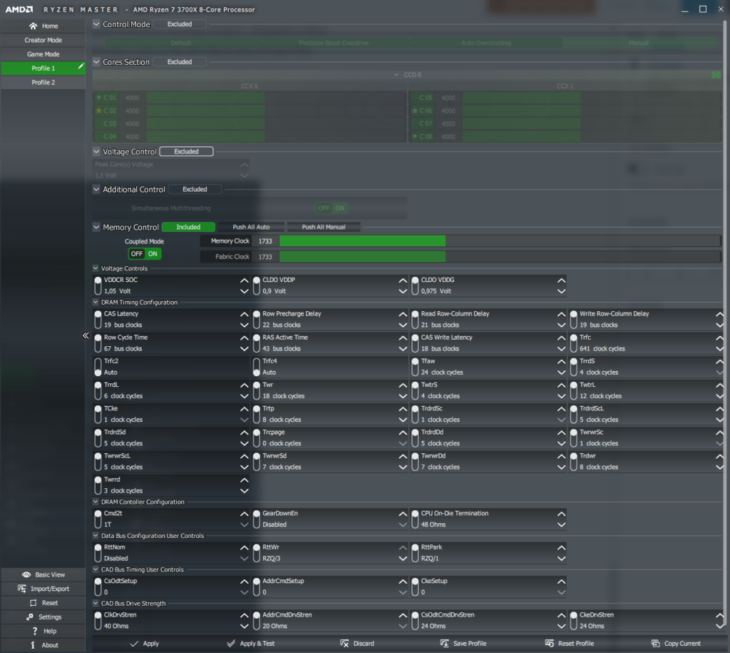
That’s it! Now save your profile and hit Apply. The XMG APEX 15 will reboot. If you do not boot successfully you need to reset your BIOS as described earlier.
Pro tip: if you plan to find the limits of your memory sticks leave the CMOS battery out. It will still boot fine, but “forget” the settings every time you unplug the AC adapter for some seconds. Not problematic in the stationary memory overclocking & testing situation. 😉
Don’t forget to excessively test your settings for stability in well-known memory test applications like Karhu Mem Test, memtest86, or TestMem5 using the 1usmus profile for example.
But it takes soo long!
Nobody said it’s easy. 😉 Take your time, have fun and good luck.
(It took roughly 3 days to find good settings for my memory sticks. Never give up.)
–
Translation of memory timings for higher DRAM frequencies (more than 3200 MT/s)
The easiest way to “translate” the timings from a lower memory frequency, for example 3200 MT/s, to 3600 MT/s is to get the multiplication factor of those both in relation. So 3600 divided by 3200 is 1.125 and if we want to find stable values to boot with a higher DRAM frequency we simply multiply them with the multiplicator we just calculated for our example.
Let’s say we got 3200 CL18-19-18-43-63 (tCAS-tRCDRd/Wr-tRP-tRAS-tRC) then our corresponding “safe” start values for 3600 MT/s would be 3600 CL20.25-21.375-20.25-48.375-70.875 respectively. Of course we can’t enter floating point numbers, so we have to round them a little. I would suggest to round them up to make sure we do not end up with tighter and possibly unstable ones straight away. So you could start with 3600 CL21-22-21-49-71 after all.
Don’t forget to translate tRFC to the higher latency too. We go from tRFC 560 to 630.
For the other timings I would suggestto go back to the safe values and start to dial them down from there.
So I would suggest to set the following timings as a starting point.
- tFAW 36
- tRRDS 6
- tRRDL 8
- tWR 24
- tWTRS 4
- tWTRL 12
- tCKe 7
- tRTP 12
- tRDRD Sc 1
- tRDRD SCL 6
- tRDRD SD 6
- tRCPage 0
- tRDRD DD 6
- tWRWR Sc 1
- tWRWR SCL 6
- tWRWR Sd 7
- tWRWR DD 7
- tRdWr 9
- tWrRd 4 (can be set to 2 or even 1 with single rank memory)
–
Results
I have tried my best with all four different memory kits and came to the following results.
After all I think it’s clear to see that dual rank (“DR” in the plots) is superior to single rank memory in most cases, even if the dual rank memory got worse timings. The ability of dual rank memory to prepare data access in parallel got a big advantage in most scenarios, especially in games with a lot of data burst / random memory access.
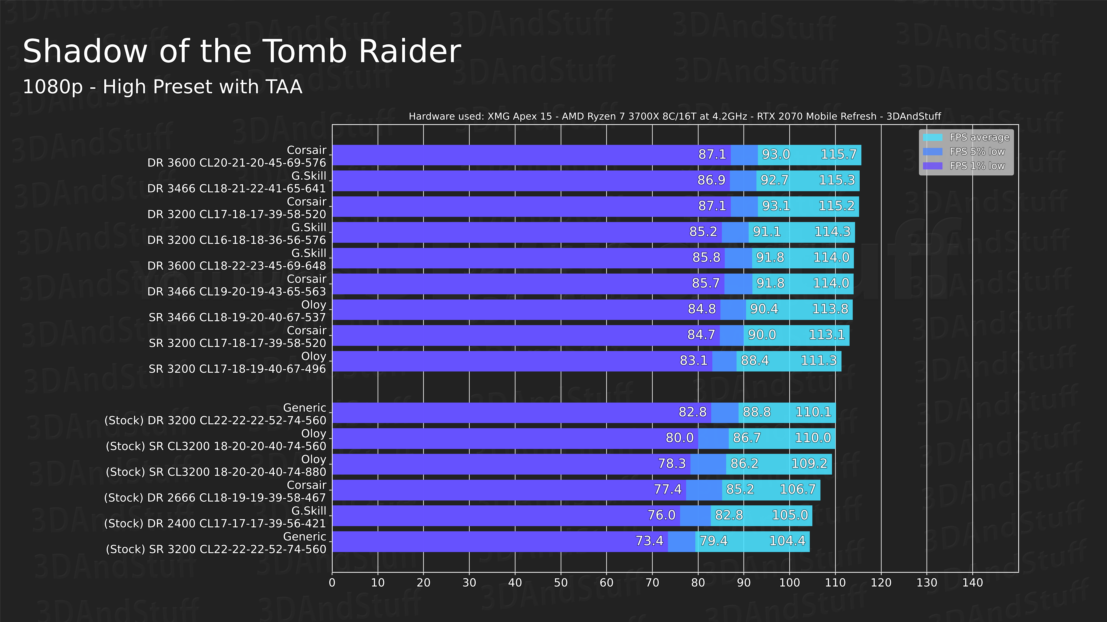
The Shadow of the Tomb Raider benchmark shows that impressively since especially the last benchmark scene is very CPU heavy. And you can gain a lot of performance with fast DRAM (tight timings) in CPU heavy situations. If the game is GPU bound, you can not really gain anything, though.
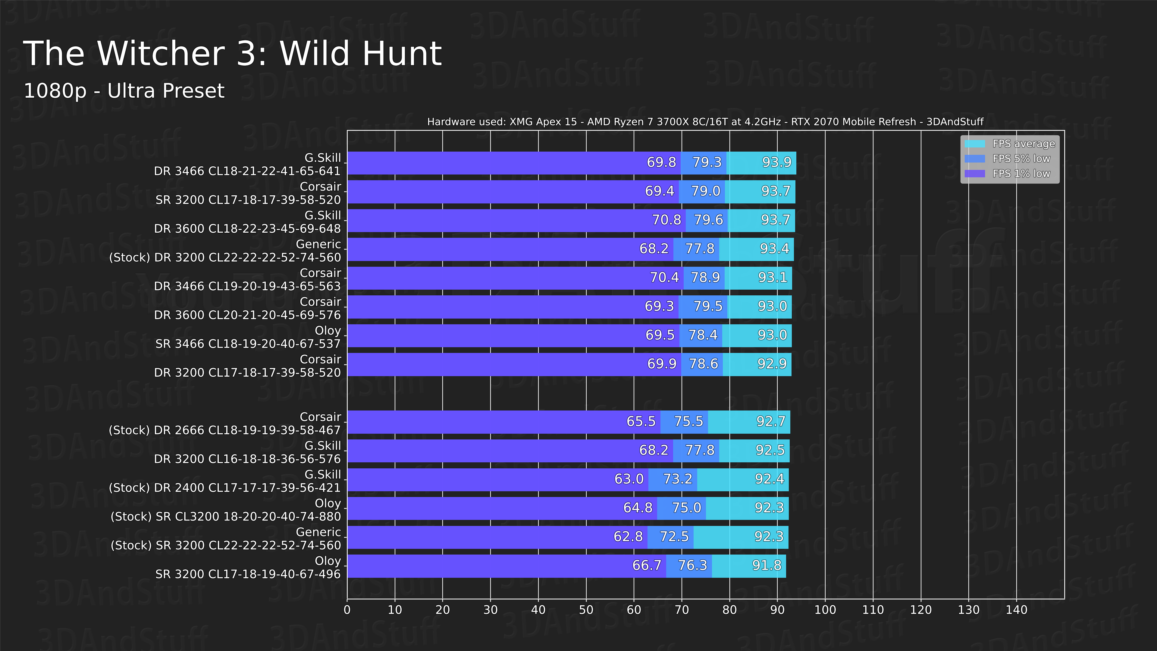
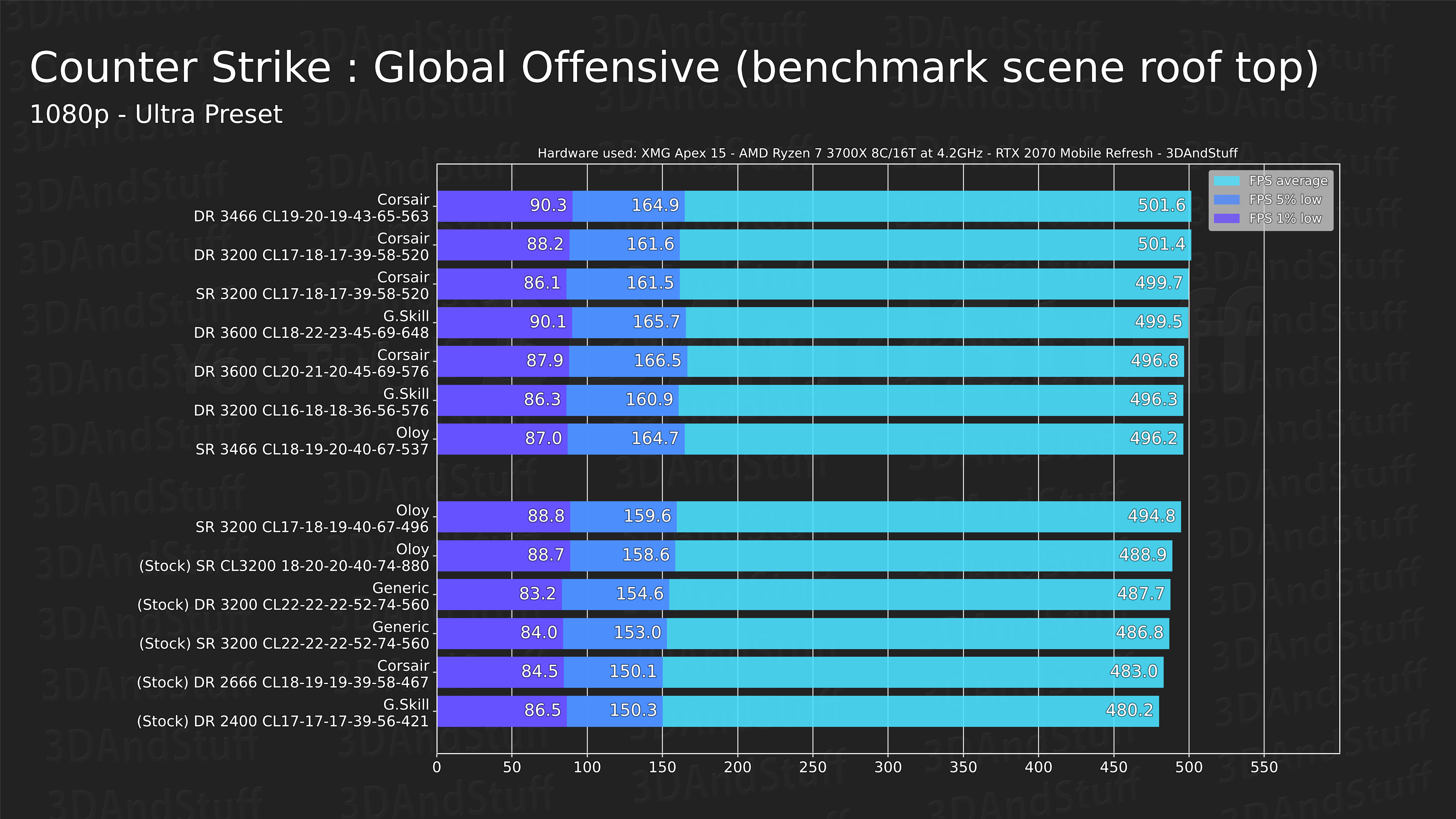
Just as the Witcher 3 shows impressively. I guess I have simply set the graphic settings with the Ultra Preset too high to run into any real CPU bottleneck. There are just minor differences. But it nicely shows that either you gain performance or not with memory overclocking is highly dependend on the use-case. Most games can make use of it though. Especially modern games. Older games like the Witcher 3, or Counter Strike : Global Offensive (CS:GO) really can’t, since they are made for older hardware with fewer CPU cores. Remember, Witcher 3 was published in 2015 and CS:GO in 2012. Those games are oldies.
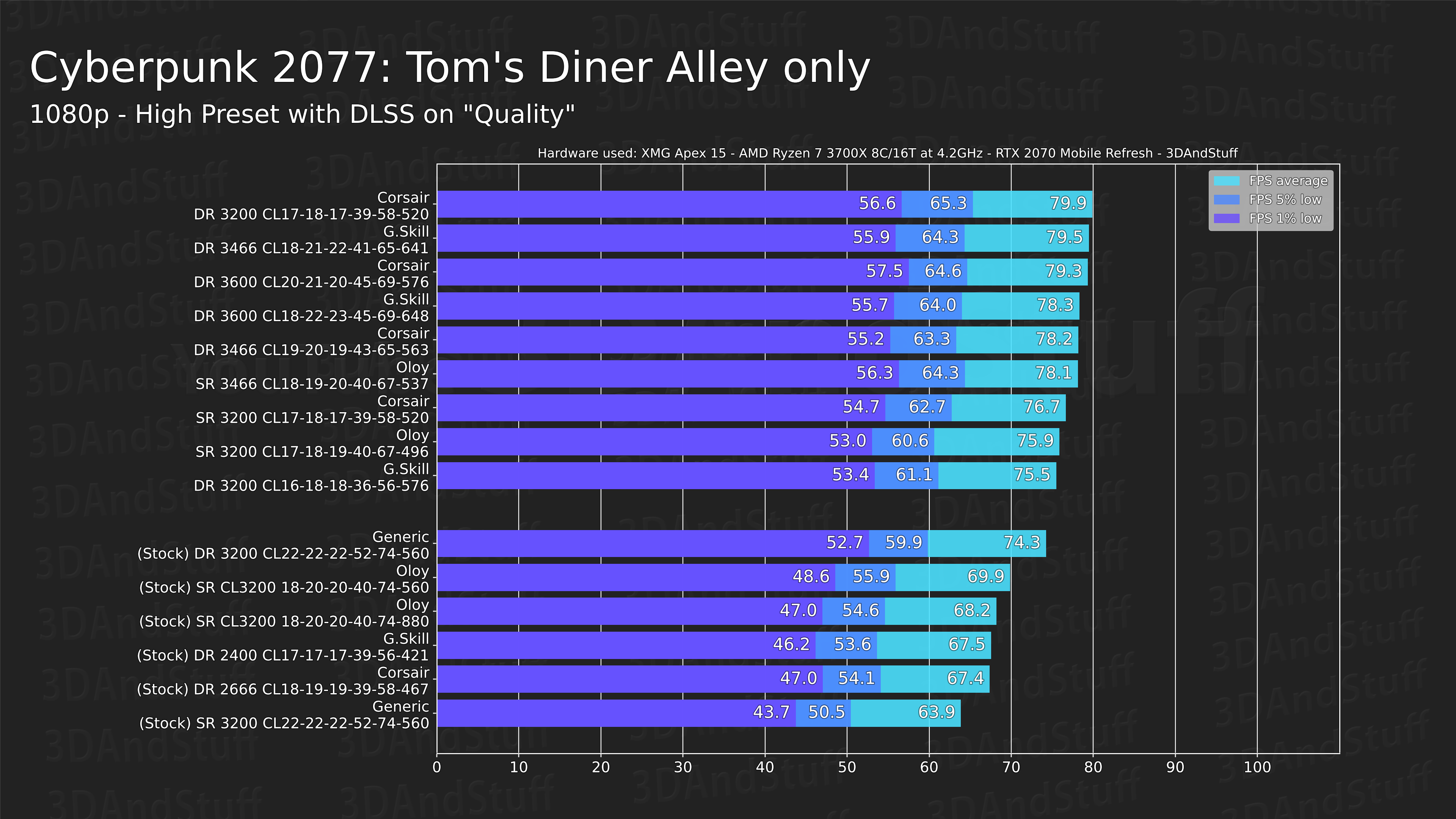
Let’s close with a modern game again. Cyberpunk 2077 can make use of many cores, especially in situations with many pedestrians and cars. I chose the many pedestrian scenario in a densly populated alley behind Tom’s Diner. But to be honest, many reviewers drive trough Night City with a car to force some high data streaming. Maybe that would’ve been a better scenario for me, too? But nevertheless, the results speak for themself.
–
End of the article.
Hope you learned something and let me know if anything stayed unclear.
Cheers

