Shunt Mod – Laptop Modding Adventure – Part 4/5
YouTube video transcription
[Original source] Partially based on the script of my YouTube videos: https://www.youtube.com/watch?v=qagEtgdVfd8
[Updated] Contains updated data from 2022.
This guide is compatible with the the following laptops.
[Laptop] XMG Apex 15 Max (2022) with B550 chipset & XMG Apex 15 (2020) with B450 chipset
[Barebone] Clevo NH50VR / NH55VR / NH57VR / NH58VR (B550) & Clevo NH50AF1 / NH55AF1 / NH57AF1 / NH58AF1 (B450)
[Similar laptops] One K56-AR, Eluktronics Thicc-15, Eurocom Nightsky ARX15
[CPU] Zen3 & Zen2 Ryzen Desktop CPUs
[Note] This guide is applicable for Zen3 and Zen2 Ryzen CPUs in the B550 chipset based XMG APEX Max (E22) and B450 chipset based XMG APEX (E20) laptop.
Hi and welcome to part 4 of the laptop GPU modding adventure.
In the parts before you saw how i soldered some wires to the I²C BUS to get temperature and power readings from the laptop’s GPU VRMs. I continued with a heatsink modification in part 3 to gain some temperature headroom on the VRMs. And finally I will present you my results of the SHUNT MOD made to my laptop’s RTX 2070 GPU in this video.
Before i start to show you the soldering process we need to talk about the stock hardware situation and also silicon quality a bit.
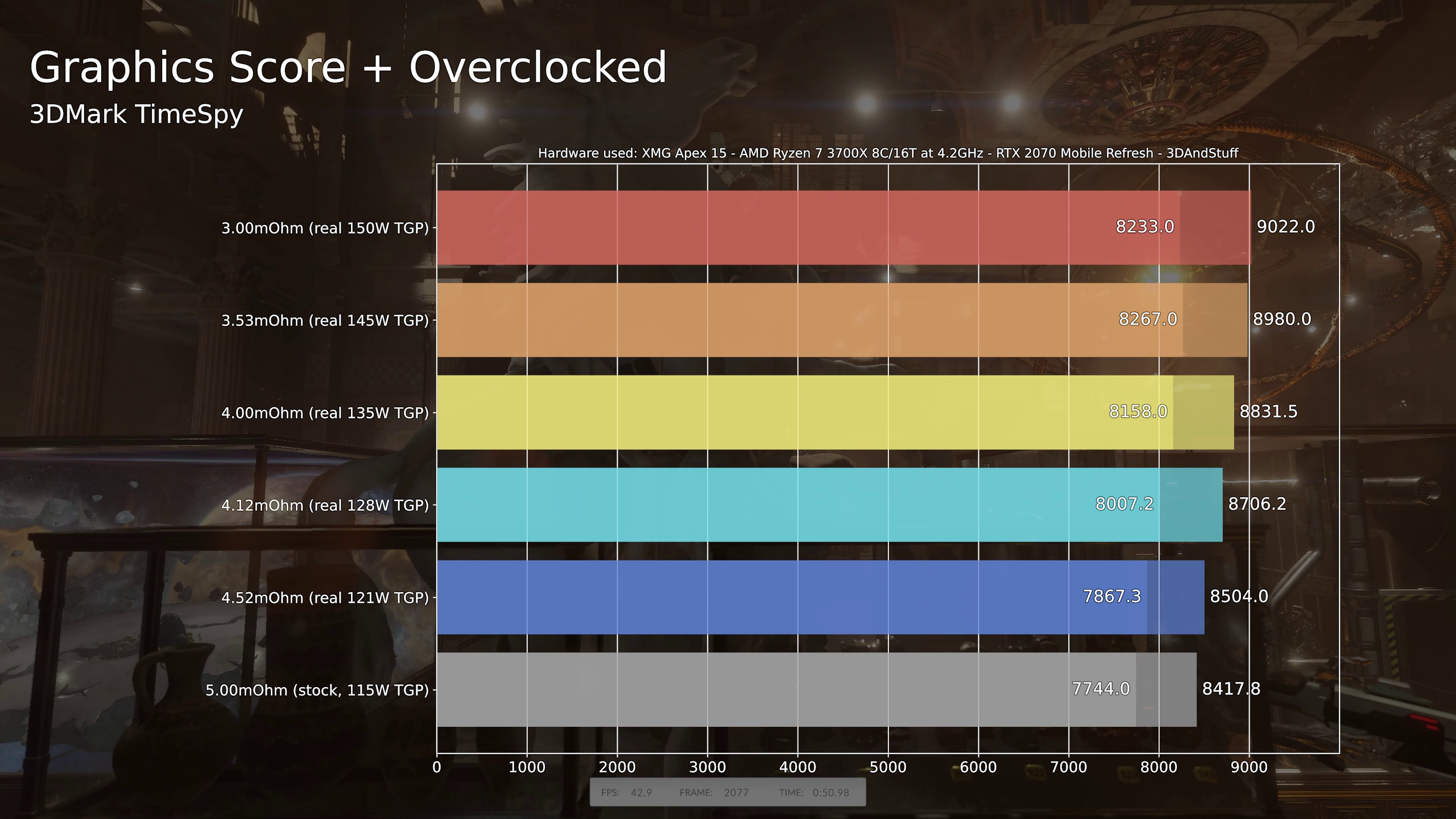
The stock 115W “RTX 2070 refresh” installed in my laptop was tested with different games and the TimeSpy benchmark. [Pause]
It achieves a graphic score between 7700 and 7800 points in TimeSpy, which is right where you would expect this laptop GPU. In the first part I said that a RTX 2070 Desktop achieves a graphics score of 9300, but an attentive subcriber of mine told me that this is only true for Factory-Overclocked-variants of the desktop RTX 2070. The regular RTX 2070 FoundersEdition does achieve a graphic score of 8700 points only. We should keep that in mind when we come to the raw non-OverClocking numbers.

Speaking of overclocking we come to the topic of silicon quality. And this is a sad one in case of my modding laptop right here. As I told you in the first video I bought the modding laptop as a spare machine without extended warranty for this video project. Comparing it to my daily laptop it turned out that the GPU’s silicon quality, .. or bin .. is not the best. It can only run a pretty under-whelming +150MHz GPU core clock in TimeSpy and up to +700MHz on the video memory until it crashes. My daily laptop can run +200 and +1000 without any hickups. That means the GPU for this project isn’t a good overclocker unfortunately, but that’s as always the risk with hardware. Welcome to silicon lottery.
Long story short, the GPU in question can provide us with an OverClocking-baseline of 8450 points in TimeSpy at best.
By the way, a friend of mine got a quite astonishing RTX 2070 GPU in his Apex15. He can run up to +250 on the GPU core and close to +1100 on the video memory, which enables him to reach more than 9000 points in TimeSpy just from simple OverClocking out of his stock 115W GPU, which is amazingly good. As we all know his grade of silicon lottery luck can only be achieved once in a lifetime. So enjoy your beast josé! 😉
https://www.3dmark.com/3dm/62004919
https://www.3dmark.com/3dm/62005095
https://www.3dmark.com/3dm/62005580
As I said in part 1 our goal will be to beat the desktop RTX 2070 (8700) and if I can also some of the factory-overclocked cards. I took the average TimeSpy graphics score of 9300 points from notebookcheck.com as reference for this extended goal.
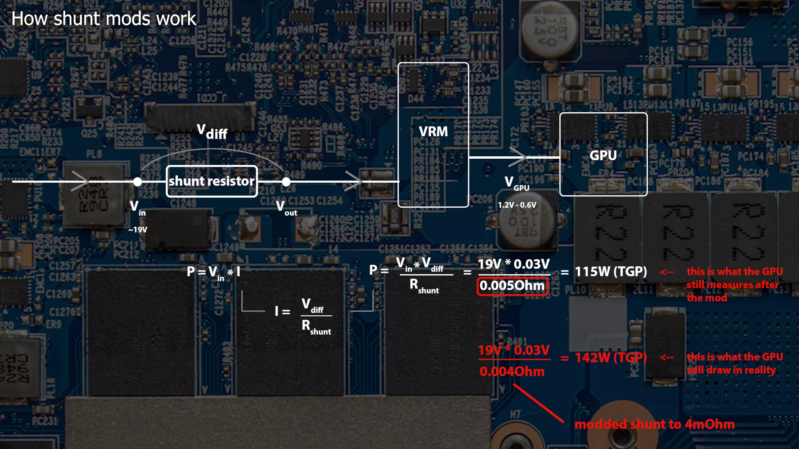


Coming to the shunts mod! The goal of a shunt mod is to increase the power draw of the GPU. Since there are power limits which can’t be exceeded you basically have to modify the power measuring circuitry.
Measuring the power draw is done by multiplying the input voltage with the current flowing trough the shunt resistor. The current can be computed by observing the voltage drop across a defined resistance, which is the shunt resistor. The higher the current the bigger the voltage drop. This way the GPU can compute the power draw and limit it’s power consumption. In our case that’s 115W TGP, which stands for “total graphics power”.
When we want to raise the power draw, but can’t simply access a power limit slider in Overclocking softwares, we need to find another way.
The easiest solution is to alter the part of the equation the GPU assumes a constant value, which is the shunt’s resistance.
After we lowered the resistance of the shunt resistor the GPU will calculate a lower overall power draw across this shunt. And because modern GPU’s are power limited it tries to fill up the missing Watts. Therefore the GPU will still report 115W power draw, but is drawing more power instead.
As a side-effect we can’t trust the power readings reported in monitoring softwares anymore. But I can make use of the i²c BUS mod I made in part two of this project to see the real power draw reported by the VRMs. The readings are quite noisy, but can be smoothed using the recorded logs later.
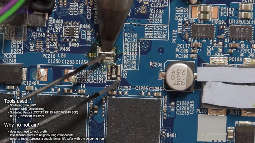
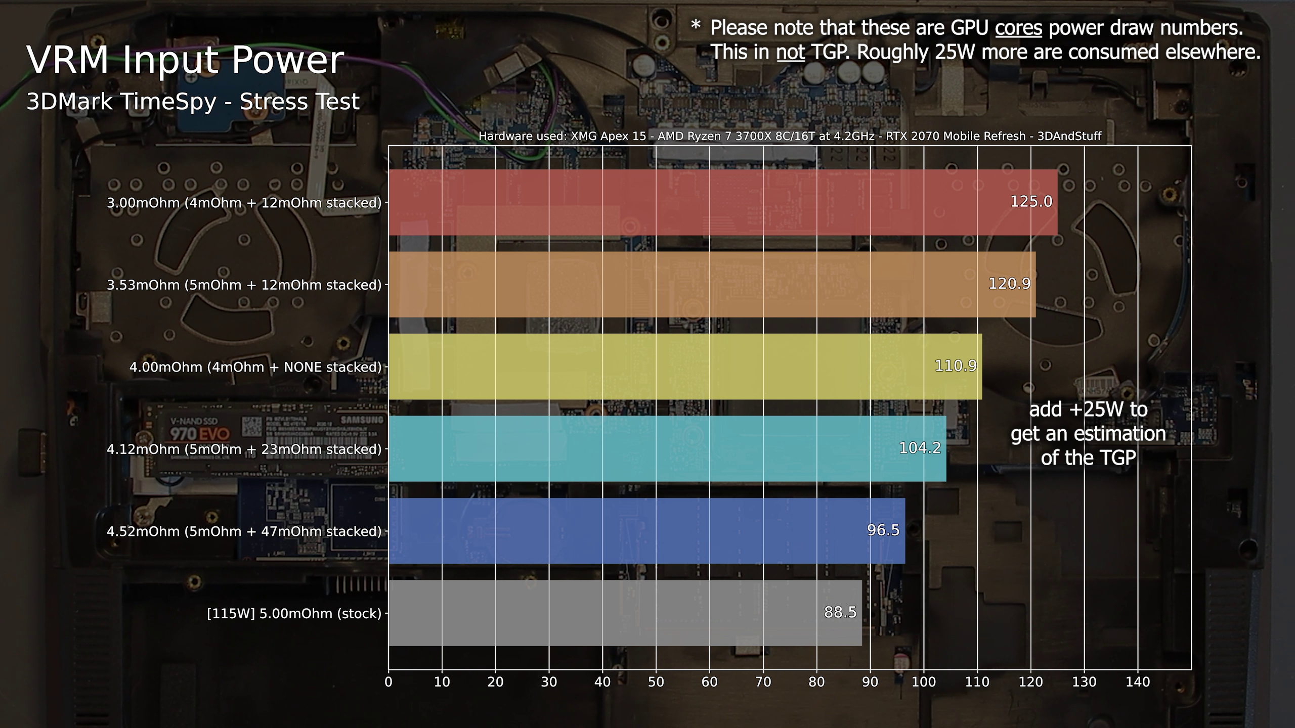
Ok now let’s take a look at the mainboard. Next to the GPU section you can see two components labeled RS1 and RS2. Those are our shunt resistors. RS1 measures the total graphics power, aka TGP, and RS2 measures the GPU core power draw only.
In our case we got an RTX 2070 with 115W TGP, so RS1 is seeing the full 115watts, while RS2 on the other hand will only see roughly 90Watts. The missing 25 Watts are consumed by the video memory and other IO stuff.

As the first stage I planned to aim for roughly 125W. But because there are no appropriate shunt resistors available I will need to stack two or three resitors on top of each other in parallel.
Using the original 5mOhms and an additional 47mOhms resistor I should be able to come in at around 4.5mOhm in total, or 127Watts.
At least I thought so…. but more after this little timelapse.
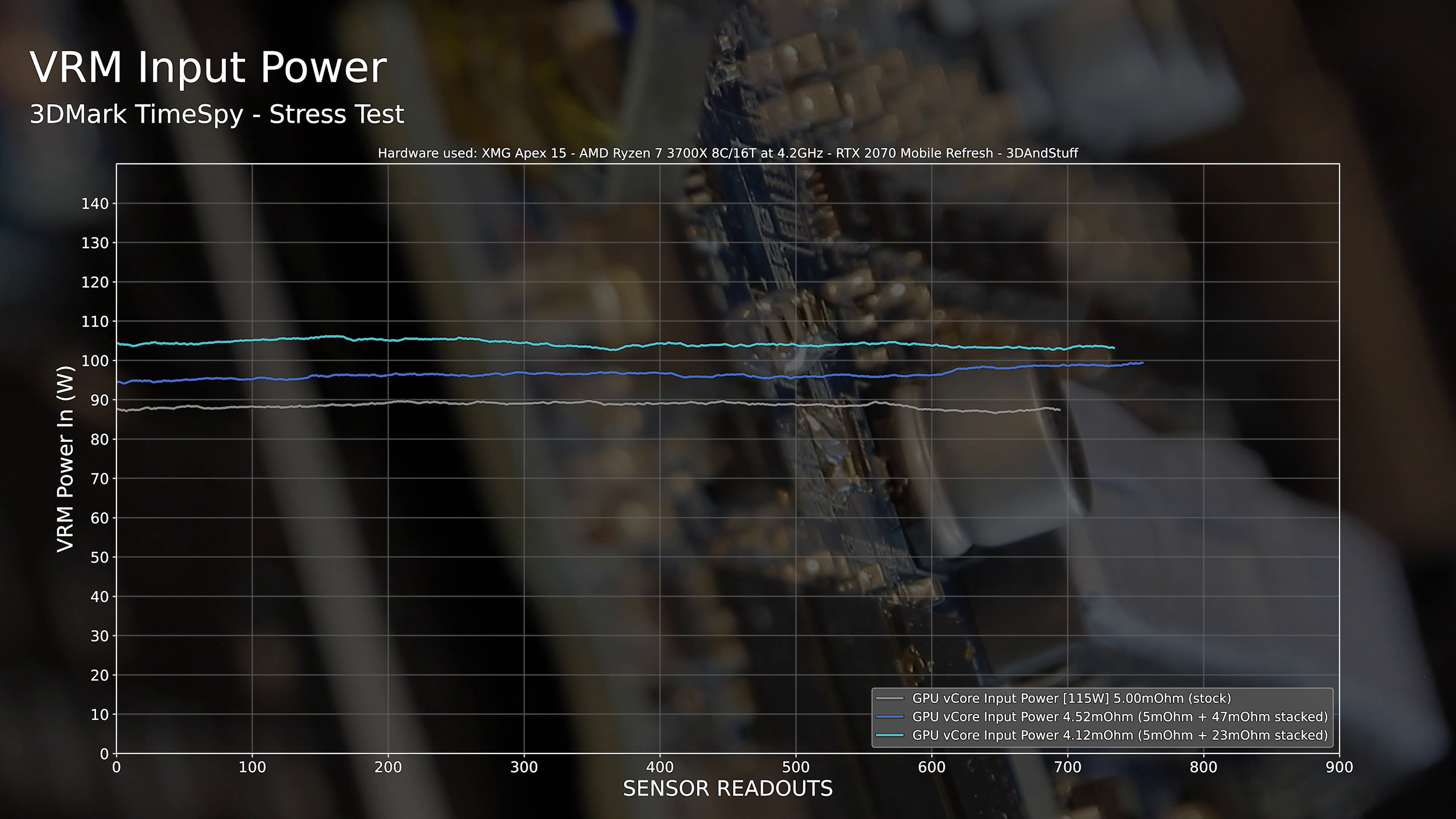
Good news is the laptop booted just fine and it got a higher score than before, but only by a very small amount. Analyzing the logged data from the VRMs showed why the score was so low. I was running at only 6W more power draw than stock. I was expecting double the increase, SO I soldered in a second 47mOhm resistor in parallel to see if we see the strange behaviour again.
At the end of this process the three stacked resistors were soldered in nicely, BUUUT do look quite funny.
The laptop booted just fine and the score was higher again. The logged data revealed that we got roughly 127 Watts using this little shunt tower. So it still is roughly half of the power draw increase I would expect.

Because I was nowhere near my 140W goal I needed to purchase some more shunt resistors. So in the end I ordered some additional 12mOhm, 5mOhm and 4mOhm ones.
Because this video will be quite long anyway I will skip any further explanations and come to the results straight away. I tried out some more combinations down to 3mOhms in total and what you can see here are the resulting real power draws of all my attempts.
What is very noticeable is that the top two configurations draw roughly the same power, which was strange since they got different resistances.
The reason for was that the second shunt was limiting both configurations. I changed the second shunt to a 47mOhm by 5mOhm configuration earlier and this turns out to be a natural limiter to around 150 Watts power draw in total. But again, it still made no sense why the first shunt behaves like this. The 5mOhm + 12mOhm combination should never reach 150W, but 140W instead according to the previous strange behaviour at 121 and 127W TGP.
The whole computations beforehand don’t match the results and I am still trying to understand why this is the case. It could be a wrongly labeled resistor involved, or the power reading circuitry is more complex than just measuring the voltage drop across the shunts.
I will try to investigate it further. But maybe one of you guys can explain what’s going on. Let me know in the comments section.
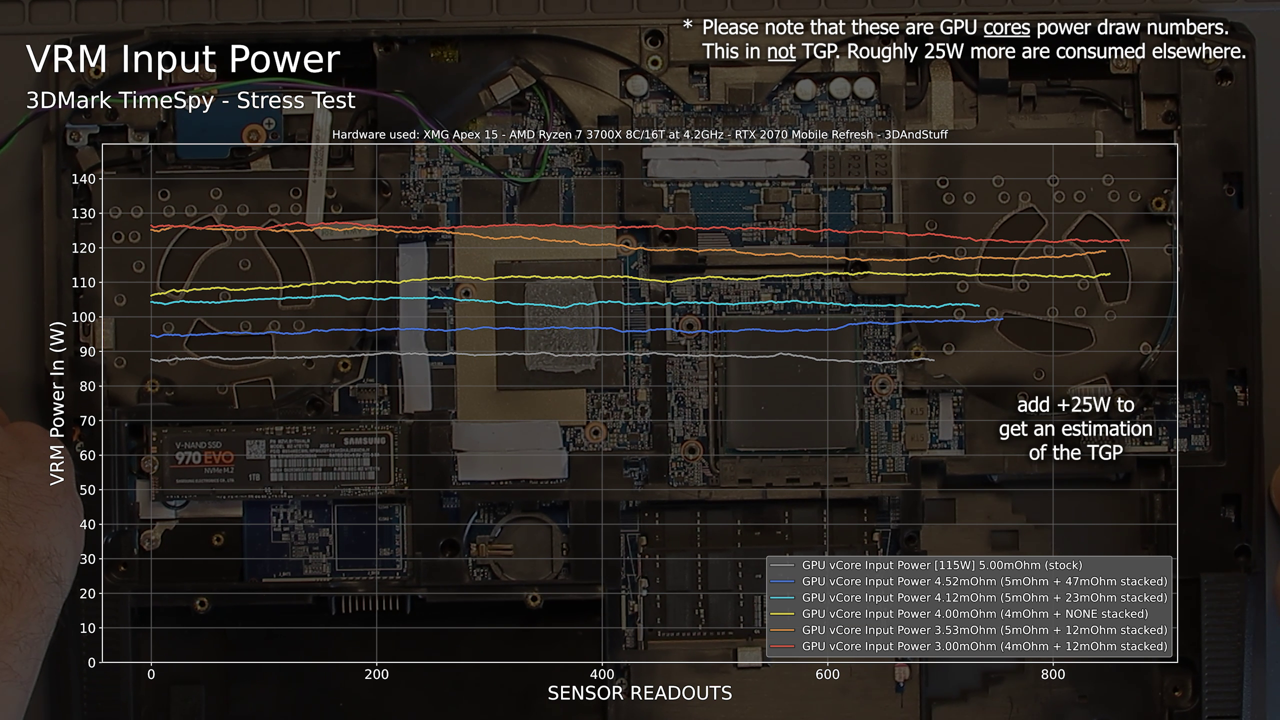


Finally let’s take a look at some interesting data I could collect. We saw the VRM power readings before, but what about it’s temperature? Is my modded heatsink I made in part 3 any good? [Pause]
Yes it is! I managed to keep the temperatures low enough to say that the VRM runs in a safe temperature range, even at 150 Watts.
And the GPU temperatue? Well, it get’s really hot! Basically the 4 mOhm shunt mod, so a total of 135 Watts, let’s the system run just under the 87°C throttle point. As soon as the GPU core hits 87°C NVidia Turing GPUs throttle down their clockspeed massively. Unfortunately that happens with the 150 Watts shunt mod after just 2 minutes into the stress test.
Of course, Raw performance improved too. But don’t expect any wonders here. Remember, the Founders Edition RTX 2070 desktop got 175 Watts and a graphics score of 8700 points in TimeSpy. Of course we stayed under 8700 points without overclocking. What hold’s us back in case of the “RTX 2070 mobile refresh” is not just the core clock, it’s also the memory clock. We run at only 11Gbps instead of the regular 14Gbps of desktop GPUs.
But Overclocking gives us some quite nice speed bumps and we can overtake the regular desktop RTX 2070 quite easily. In fact we come close to some factory-OC variants, but are still some points away from the average 9300 points as seen with desktop OC cards.
In Cyberpunk 2077 our performance improved slightly over the stock RTX 2070 mobile.
So it did in the “Witcher 3” and “Shadow of the Tomb Raider”, but only if we are not running into a CPU limit.
Lastly I want to show you my attempt to break the record of the “RTX 2070 mobile refresh” in TimeSpy. I know it seems to be a bit unfair, but all the leading scores on those leaderboards are made under not very practical conditions. So i guess my run was still quite… NORMAL? Not sure though hehe. The score I ended with was a graphics score of exactly 9300 points. Which was my initial goal to beat. So I did it technically. Even if the conditions are anything but normal. You can find the link to some of these runs in the video description.
After all the effort I wish my GPU would have been a better bin. A graphics score of 9300 points is pretty much the best my GPU can achieve. There should be plenty of better bins out there which could hit more than 9500 points easily.
Let’s see and wait for another RTX 2070 Mobile Refresh laptop owner attempt a shunt mod and proof my guess to be true.

I got so much more data than just the ones shown. So if you have any question or miss some informations, let me know in the comments. I will update the data for you.
And I guess the next part will be the final one for this project. If everything works according to plan I will sand down and polish the surfaces of the modified heatsink and will bring it to a company which will nickel plate it professionally. With the nickel plated heatsink I want to try out liquid metal in this laptop and investigate in which way the temperatures and performance improves.

